

Description
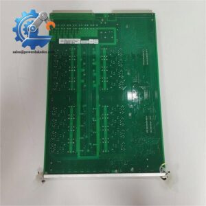
- LAM 810-099175-012 | Semiconductor Process Tool Replacement PCB
2. At-A-Glance Executive Brief
- Model: LAM 810-099175-012
- Brand: Lam Research
- Series: VIOP Phase III / VME Control Platform
- Part Type: Analog I/O Interface PCB Assembly
- Core Function: Processes analog field signals between semiconductor process equipment subsystems and the VME-based control architecture.
- Primary Use: Lam Research semiconductor fabrication equipment, including legacy etch and deposition process platforms.
- Key Specifications:
- VMEbus-based industrial PCB design
- Analog signal acquisition and interface capability
- Designed for semiconductor manufacturing equipment control
- Board-level replacement spare for installed process tools
- Typical Deployment: Wafer fabrication equipment cabinets, process control racks, and legacy Lam Research platforms.
3. Product Introduction
Inside a Lam Research semiconductor process tool, the 810-099175-012 functions as a VIOP Phase III interface board that connects analog measurement and control signals with the equipment control system. This board operates within a VME-based architecture where precise signal conversion and communication stability are required for chamber monitoring, process control, and equipment sequencing.
In field deployments, engineers typically handle this PCB as a critical production spare because analog interface failures can interrupt wafer processing even when mechanical assemblies remain functional. Verify the board revision, installed software configuration, VME slot assignment, and connected harnesses before replacement (a mismatch can create false process alarms after installation).
4. Core Technical Specifications
| Parameter | Value |
|---|---|
| Manufacturer | Lam Research |
| Part Number | 810-099175-012 |
| Board Type | VIOP Phase III PCB Assembly |
| Functional Category | Analog Input / Output Interface Board |
| System Architecture | VMEbus Control Platform |
| Application | Semiconductor Manufacturing Equipment |
| Signal Processing | Analog field signal acquisition and interface |
| Installation Method | VME rack slot mounting |
| Backplane Interface | VME bus connector |
| PCB Construction | Industrial multi-layer circuit board |
| Operating Environment | Semiconductor equipment cabinet |
| Cooling Method | Forced cabinet airflow |
| Weight | Approx. 0.25–1 kg depending on assembly configuration |
| Compatible Equipment | Lam Research legacy process tools |
| Storage Requirement | ESD-controlled environment |
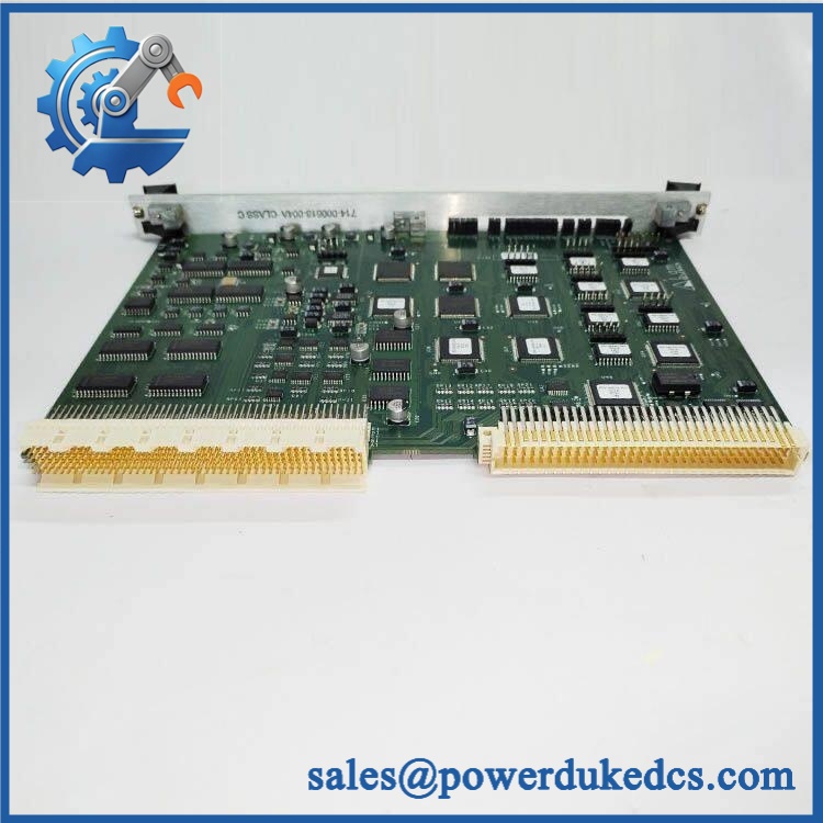
LAM 810-099175-012
5. Application Scenarios & Pain Points
A failed analog interface board can create inaccurate sensor feedback, causing a process chamber to stop even when the main controller remains online.
- Wafer etch equipment: The board supports analog feedback paths used for process monitoring, where unstable signals can affect pressure, temperature, or flow control loops.
- Deposition systems: During thin-film processing, accurate analog feedback is required to maintain repeatable chamber conditions.
- Legacy Lam Research platforms: Facilities operating older VME-based tools often maintain spare PCB assemblies because full system migration requires significant engineering validation.
- High-volume semiconductor fabs: A single failed interface board can delay production recovery during a scheduled maintenance window lasting only a few hours.
- Equipment refurbishment programs: Used and new-surplus boards are commonly evaluated as replacement options when OEM supply channels are limited.
6. Common Error Codes & Diagnostic Symptoms
Symptom/Code: Analog Channel Reading Fixed at 0V or Full Scale
→ Diagnosis: Possible analog input circuit failure, damaged signal conditioning components, or connector contact problems.
→ Action: Inspect field wiring and replace the 810-099175-012 board if the channel hardware fails verification.
Symptom/Code: VME Communication Fault / Board Not Detected
→ Diagnosis: Possible VME backplane connection issue, board processor/interface fault, or slot configuration problem.
→ Action: Reseat the board, inspect connectors, and replace the PCB if communication remains unavailable.
Symptom/Code: Process Alarm After Sensor Replacement
→ Diagnosis: Analog scaling mismatch, calibration data loss, or unstable signal conversion.
→ Action: Verify equipment configuration and replace the interface board if conversion accuracy is outside limits.
7. Cross-Reference & Lifecycle Migration
- Related Versions:
- LAM 810-099175-009
- LAM 810-099175-011
These variants belong to the same VIOP board family but may differ by hardware revision and equipment compatibility.
- Replacement Considerations:
- Confirm exact Lam equipment model.
- Verify VME slot location.
- Match board revision.
- Confirm software compatibility.
- Firmware / Configuration:
Board replacement may require equipment calibration, configuration verification, or parameter restoration depending on the installed process tool. - Lifecycle Status: Legacy / Limited Availability
- Still required for installed semiconductor manufacturing equipment.
- Recommended stock strategy: maintain tested spare boards for production-critical tools.
8. Field Engineer’s Tech Notes (Anti-Pitfall Guide)
- Do not install the board without recording the original slot position.
VME systems depend on correct hardware placement and configuration. A physically compatible board installed in the wrong location may not initialize correctly. - Handle the edge connectors carefully.
Semiconductor equipment environments can expose contacts to chemical residues. Inspect gold fingers and clean only with approved methods before installation (minor oxidation can create intermittent faults).
9. Strict QA & Testing SOP
Step 1 — Incoming Inspection
- Confirm part number: LAM 810-099175-012.
- Record serial number, revision marking, and board labels.
- Inspect PCB surface, connectors, and components.
- Photograph received condition.
Step 2 — Electrical Inspection
- Verify power rail condition.
- Check for damaged capacitors, burned components, or contamination.
- Confirm connector continuity.
Step 3 — VME Functional Testing
- Install into compatible VME test environment.
- Verify board recognition.
- Check communication stability.
Step 4 — Analog Signal Testing
- Apply simulated analog inputs.
- Verify signal conversion response.
- Check channel stability over runtime.
Step 5 — Packaging Control
- Place the PCB inside ESD shielding packaging.
- Add moisture protection where required.
- Protect connectors during shipment.
Test videos are available for verified inspection records.
10. Buyer’s FAQ (Dynamic Q&A)
Q: Can the LAM 810-099175-012 be replaced while the semiconductor tool is running?
A: No. This board is part of the equipment control architecture, and removal during operation can interrupt process control signals. Follow the machine manufacturer’s maintenance procedure.
Q: How can I confirm this is an original Lam Research 810-099175-012?
A: Verify the Lam label, part number, PCB markings, revision information, connector condition, and inspection records. Board-level semiconductor spares should have traceable testing documentation.
Q: Does this board require software loading after replacement?
A: The PCB itself is not normally programmed like a PLC CPU. However, equipment calibration, configuration files, and process parameters may need verification after installation.
Q: What warranty should be requested when purchasing this spare board?
A: Confirm whether the supplier provides functional testing, inspection photos, replacement coverage, and transit protection. For semiconductor equipment parts, documented test evidence is an important purchasing factor.



 Start Chat