

Description
- LAM 810-800081-022 | New Surplus Process Control Card
2. At-A-Glance Executive Brief
- Model: LAM 810-800081-022
- Brand: LAM Research
- Series/System: Lam Semiconductor Etch Equipment Platform
- Part Type: P2MB VME PCB Assembly / Etch Control Interface Board
- Core Function: Provides control and interface functions within Lam Research semiconductor processing equipment, supporting communication and signal exchange between equipment subsystems.
- Key Specs:
- PCB Assembly identification: P2MB.V ME.ETCH
- Designed for Lam etch process equipment
- VME-based hardware architecture
- Industrial semiconductor equipment spare component
- Used in legacy Lam Research platforms requiring lifecycle support
3. Product Introduction
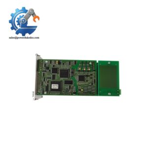
A semiconductor production line can lose valuable wafer-processing capacity when an aging control board causes equipment communication faults or prevents chamber initialization. The LAM 810-800081-022 is a dedicated PCB assembly used inside Lam Research semiconductor manufacturing equipment, serving as a hardware interface component within the equipment control architecture. It is identified by suppliers as PCB ASSY P2MB.V ME.ETCH and is associated with Lam etch process platforms.
Installed inside the equipment electronics system, this board interfaces with the machine control framework rather than operating as a standalone PLC module. Before replacement, verify the exact tool model, board revision, connector arrangement, and system configuration. A matching part number is essential, but semiconductor equipment often requires revision-level confirmation before installation (—especially for older etch platforms maintained through spare inventory programs).
4. Core Technical Specifications
| Parameter | Value |
|---|---|
| Manufacturer | LAM Research |
| Model Number | 810-800081-022 |
| Assembly Identification | PCB ASSY P2MB.V ME.ETCH |
| Product Type | Semiconductor equipment PCB assembly |
| Application | Etch process equipment |
| Hardware Architecture | VME-based control system interface |
| PCB Construction | Multi-layer industrial PCB |
| PCB Material | FR4 high-temperature laminate (reported) |
| Connector Interface | VME / equipment-specific backplane connection |
| Mounting Method | Internal equipment chassis installation |
| Function | Equipment control and signal interface |
| Operating Environment | Semiconductor manufacturing equipment enclosure |
| Cooling Method | Equipment internal airflow system |
| Weight | Approx. 2–3 kg range depending on assembly configuration |
| Replacement Type | Direct hardware spare (configuration verification required) |
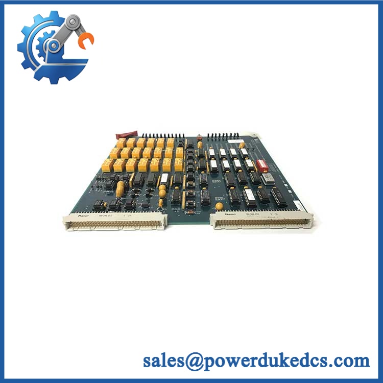
LAM 810-800081-022
5. Application Scenarios & Pain Points
When an etch tool fails to complete initialization, the control PCB becomes one of the first hardware checkpoints. The 810-800081-022 is typically maintained for equipment recovery situations where production continuity matters.
- Semiconductor wafer etching: Supports control electronics inside Lam etch platforms where process parameters must remain stable during plasma processing.
- Legacy equipment maintenance: Helps extend operational life for installed Lam systems where OEM replacement cycles are limited.
- High-volume semiconductor fabs: Used as a spare asset to reduce downtime during scheduled or unexpected equipment failures.
- Equipment refurbishment projects: Applied during restoration of used semiconductor processing tools before factory acceptance testing.
- Process development laboratories: Supports older Lam equipment retained for specialized process development.
A modern semiconductor fab may calculate equipment downtime in thousands of dollars per hour, making verified spare PCB availability an important maintenance consideration.
6. ? Common Error Codes & Diagnostic Symptoms
Symptom/Code: Equipment controller fails during startup initialization
→ Diagnosis: Possible PCB communication failure, damaged VME interface, or unstable board-level electronics.
→ Action: Verify power and backplane connection, then replace 810-800081-022.
Symptom/Code: Intermittent chamber communication loss
→ Diagnosis: Possible connector degradation, signal integrity issue, or aging PCB components.
→ Action: Inspect connectors and replace the board if communication instability follows the module.
Symptom/Code: Tool hardware configuration mismatch after replacement
→ Diagnosis: Possible revision difference or incompatible board configuration.
→ Action: Confirm revision compatibility before installation.
7. Cross-Reference & Lifecycle Migration
- Compatibility Notes:
- LAM 810-800081-022 is associated with Lam Research semiconductor equipment platforms.
- Replacement requires confirmation of:
- Equipment model
- PCB revision
- Installed software configuration
- Connector layout
- Previous / Related Versions:
- Related Lam VME PCB assemblies may exist with similar numbering structures, but direct substitution should not be assumed.
- Firmware / Configuration Requirements:
- This PCB assembly is not normally programmed like a PLC CPU.
- Equipment software recognition and hardware configuration checks may be required after replacement.
- Lifecycle Status:
- Status: Legacy / Limited Availability
- Maintain tested spare stock for older Lam tools because semiconductor equipment often remains productive long after original hardware release cycles.
- Migration Strategy:
- Record board revision before removal.
- Archive equipment configuration information.
- Keep one verified spare for critical production tools.
8. Field Engineer’s Tech Notes (Anti-Pitfall Guide)
- Do not handle the PCB without ESD protection.
Semiconductor equipment boards contain sensitive electronic components. Always use a grounded wrist strap and approved ESD packaging during replacement. - Do not assume connector condition is acceptable.
Inspect the VME interface and backplane contacts carefully. Oxidation or contamination can create symptoms that appear to be a failed PCB.
9. Strict QA & Testing SOP
A controlled quality process for LAM 810-800081-022 should include:
Step 1 — Incoming Inspection
- Verify LAM label and complete part number.
- Record serial number and revision marking.
- Inspect PCB surface and connector condition.
Step 2 — Physical Examination
- Check for:
- Burn marks
- Capacitor leakage
- Bent pins
- PCB damage
- Contamination
Step 3 — Electrical Testing
- Verify power input behavior.
- Check current consumption.
- Inspect communication interface response.
Step 4 — Functional Testing
- Install into compatible Lam equipment test environment where available.
- Verify startup communication.
- Confirm board recognition.
- Check system diagnostics.
Step 5 — Packaging Control
- Place PCB inside anti-static shielding packaging.
- Use shock protection for international transport.
- Maintain inspection records.
Test videos are available for selected inspected units.
10. Buyer’s FAQ (Dynamic Q&A)
Q: Can the LAM 810-800081-022 be hot-swapped?
A: Do not assume hot replacement capability. Semiconductor process equipment normally requires controlled shutdown procedures before removing internal PCB assemblies.
Q: How do I verify this is a genuine LAM Research spare?
A: Confirm the board label, complete part number, revision marking, physical PCB layout, and supplier traceability documentation. Part-number matching alone may not confirm equipment compatibility.
Q: Does this PCB require firmware loading after installation?
A: Typically, this type of equipment PCB is not configured like a PLC CPU. However, Lam equipment software may require hardware recognition checks or configuration validation after replacement.
Q: What warranty is available for this board?
A: Warranty depends on supply condition. Confirm whether the unit is new original, unused surplus, refurbished, or tested before purchase. Request inspection records and warranty terms with the quotation.




 Start Chat