

Description
- LAM 810-046015-010 | Factory Tested Semiconductor Hardware
2. At-A-Glance Executive Brief
- Model: LAM 810-046015-010
- Manufacturer: Lam Research
- Series: Semiconductor Process Equipment Control Hardware
- Part Type: VIOP III PCB Board / Control Circuit Assembly
- Core Function: Provides electronic interface and control signal processing functions inside Lam Research semiconductor manufacturing equipment.
- Key Specifications:
- VIOP III board assembly.
- Used in Lam Research wafer processing equipment.
- PCB-based electronic control assembly.
- Designed for precision semiconductor manufacturing environments.
- Supports equipment-level communication and control functions.
- Typical Procurement Category: Semiconductor capital equipment spare, OEM process tool replacement PCB, cleanroom maintenance inventory.
3. Product Introduction
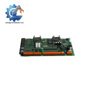
Inside a Lam Research semiconductor process tool, the 810-046015-010 VIOP III PCB assembly functions as an equipment-level electronic control interface. When this type of board fails, the impact can appear as process interruptions, communication faults, abnormal subsystem behavior, or inability to complete wafer processing sequences. In field deployments, engineers normally inspect the PCB, cable harnesses, power rails, and connected assemblies together because semiconductor equipment faults often involve multiple hardware layers.
The 810-046015-010 is identified in the aftermarket as a Lam Research VIOP III board assembly used in semiconductor manufacturing equipment. Exact tool compatibility depends on the installed Lam platform, board revision, and machine configuration. Before replacement, confirm the equipment model, firmware environment, and stored calibration information (critical for maintaining process repeatability).
4. Core Technical Specifications
| Parameter | Value |
|---|---|
| Manufacturer | Lam Research |
| Part Number | 810-046015-010 |
| Board Type | VIOP III PCB Assembly |
| Product Category | Semiconductor Equipment Control PCB |
| Application | Wafer fabrication process equipment |
| Equipment Platform | Lam Research process tools |
| PCB Construction | Multi-layer industrial PCB |
| Interface Type | Equipment-specific electrical interfaces |
| Installation Method | Internal equipment chassis mounting |
| Material | FR4 PCB substrate |
| Connector Interface | Multi-pin board connectors |
| Operating Environment | Semiconductor cleanroom equipment |
| Cooling Method | Equipment internal airflow |
| Configuration Data | Tool-dependent |
| Firmware Dependency | Equipment controller dependent |
| Weight | Approx. 0.3–0.5 kg depending on packaging revision |
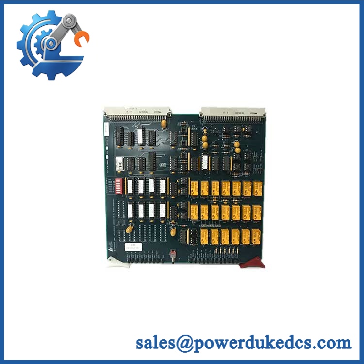
LAM 810-046015-010
5. Application Scenarios & Pain Points
At a semiconductor fabrication facility, a failed VIOP III board can stop a process module from completing wafer runs, creating equipment downtime during high-value production cycles.
For plasma etch and wafer processing systems, this PCB assembly supports internal equipment communication and control functions where signal integrity is essential.
During preventive maintenance activities, technicians often replace aging electronic assemblies before intermittent failures affect production stability.
In older Lam Research tool fleets, maintaining tested spare PCBs helps fabs continue operating legacy equipment without immediate platform migration.
Without a verified replacement board, troubleshooting may extend because identical symptoms can originate from power supplies, harnesses, controllers, or the PCB itself.
6. Common Error Codes & Diagnostic Symptoms
Symptom/Code: VIOP communication fault / board not detected
→ Diagnosis: Possible PCB communication failure, damaged connector interface, or controller bus interruption.
→ Action: Inspect connectors and replace the 810-046015-010 board if communication failure remains.
Symptom/Code: Process module initialization failure
→ Diagnosis: The control board may not complete startup communication with associated equipment subsystems.
→ Action: Verify power and cables, then replace the PCB assembly if hardware failure is confirmed.
Symptom/Code: Intermittent equipment alarms after warm-up
→ Diagnosis: Possible thermal stress, aging components, or marginal solder/connector conditions.
→ Action: Replace the board after confirming environmental and electrical conditions.
7. Cross-Reference & Lifecycle Migration
- Compatible Platform: Lam Research semiconductor manufacturing equipment.
- Related Hardware Identification: Market references commonly identify this part as a VIOP III PCB Board / VIOP-3 Board.
- Replacement Considerations:
- Match exact part number.
- Verify PCB revision.
- Confirm equipment model compatibility.
- Compare connector layout before installation.
- Firmware Requirement: Firmware and configuration are typically managed by the host equipment controller. Board replacement may require system-level verification or configuration restoration.
- Lifecycle Status: Legacy / Controlled Spare.
- Maintain tested inventory for installed Lam tools.
- Store with equipment model, serial information, and previous board revision records.
8. Field Engineer’s Tech Notes (Anti-Pitfall Guide)
- Do not install the PCB without recording the original board revision.
Semiconductor equipment may use multiple revisions with similar external markings but different electrical characteristics. - Never handle the board without ESD protection.
Semiconductor tool electronics can contain sensitive components that fail from static discharge without visible damage. - Inspect connector seating carefully.
A partially engaged multi-pin connector can create symptoms identical to a failed PCB.
9. Strict QA & Testing SOP
Step 1 — Incoming Inspection
- Verify Lam Research label and part number.
- Confirm 810-046015-010 marking.
- Record serial number and revision information.
- Photograph PCB condition.
Step 2 — Physical Examination
- Inspect PCB surface.
- Check connectors and pins.
- Look for oxidation, contamination, or mechanical damage.
Step 3 — Electrical Inspection
- Verify board power input paths.
- Check connector continuity.
- Inspect critical components.
Step 4 — Functional Testing
- Install into compatible Lam test equipment when available.
- Verify board recognition.
- Check communication response.
- Confirm operational status.
Step 5 — Packaging Control
- Place PCB inside ESD shielding packaging.
- Use moisture and shock protection.
- Attach inspection documentation.
Test videos are available for verification procedures when required.
10. Buyer’s FAQ (Dynamic Q&A)
Q: Can the Lam 810-046015-010 PCB be replaced while the process tool is powered?
A: No. Shut down the equipment according to the Lam maintenance procedure. Removing or inserting PCB assemblies under power may damage connectors or connected electronics.
Q: How do I verify a genuine Lam Research 810-046015-010 board?
A: Confirm the Lam label, part number, PCB markings, revision information, photographs, and supplier inspection records. Semiconductor spare boards require traceable handling history.
Q: Does this PCB include the complete machine software?
A: No. The board is hardware only. Tool software, recipes, calibration data, and configuration files remain associated with the host equipment system.
Q: What warranty information should be requested before purchase?
A: Request test records, inspection photos, operating condition details, and warranty terms. For semiconductor equipment boards, functional verification is more important than visual condition alone.
Procurement Note: The Lam Research 810-046015-010 should be managed as a controlled semiconductor equipment spare. Keep PCB revision data, equipment compatibility records, and test documentation together to reduce recovery time during production interruptions.




 Start Chat